Electron Beam Lithography System Market
Electron Beam Lithography System Market Size, Trends, Opportunity, and Forecast Analysis, 2026-2036
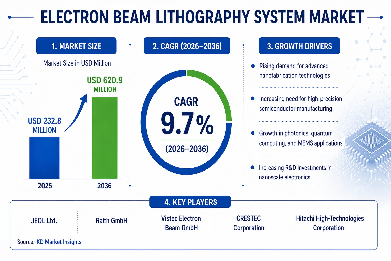
Electron beam lithography system market revenue to generate USD 620.9 million by 2036, according to KDMI analyst’s growth analysis. The market is segmented by component, end use, technology, price, application, and region.
Key Highlights
- 2025 Market Size: USD 232.8 Million
- 2036 Forecast Market Size: USD 620.9 Million
- CAGR (2026–2036): 9.7%
- Largest Market: Asia-Pacific is the largest regional market, accounting for around 35–36% share.
- Fastest Growing Region: Asia-Pacific is also the fastest-growing region.
- Key Market Drivers: Rising demand for miniaturization of electronic devices and nanoscale fabrication.
- Key Players: Raith GmbH, JEOL Ltd., Vistec Electron Beam GmbH, Elionix Inc., CRESTEC Corporation, and NanoBeam Ltd.
Electron Beam Lithography System Market Size Report – In a Glance
As per the survey report on Electron beam lithography system market, the market is expected to foresee a CAGR value of 9.7% during 2026-2036, and further generate a market size of USD 620.9 million by the end of 2036. In 2025, the market size was value at USD 232.8 million revenue.
- The Electron beam lithography system market’s growth is driven by rising demand for advanced nanofabrication in electronics sector.
- In Japan, the electron beam lithography system market growth is attributed by rising demand for high-precision semiconductor manufacturing.
- KDMI analyst’s growth analysis foresees high system cost and shortage of skilled professionals as the restraint for Electron beam lithography system market.
- North America, having the highest market share in the electron beam lithography system market, is estimated to dominate the global market.
Electron Beam Lithography System (EBL) Market Analysis
An electron beam lithography system uses a focused electron beam to draw high-resolution patterns on a substrate coated with an electron-sensitive film called a resist. This beam changes solubility of the resist, and create nanoscale structures after removing exposed or unexposed areas by using a solvent. This process is performed for applications demanding ultra high-resolution and is valuable for mask fabrication, low-volume semiconductor manufacturing and nanotechnology research. The demand for EBL system across the leading industries such as telecommunications, consumer electronics, aerospace and defense. According to the NIH report, the global nanotechnology market is expected to reach USD 306.1 billion in 2025, which has experienced a significant increase from 2018 value of USD 160.8 billion, at a CAGR of 9.6% from 2018-2025. Nanoparticles of the industry constitutes of 85% of the overall industry. In 2021, under the budget plan - the United Stated allocated over USD 1.7 billion for the National Nanotechnology Initiative. The significant expansion of nanotechnology industry further boosts requirement of EBL system to efficiently perform research purpose.
Analysts Observation on Japan Electron Beam Lithography System (EBL) Market Survey
The Japan electron beam lithography system market growth is driven by the growing demand for high-precision semiconductor manufacturing and advanced nanofabrication technologies. As the Japanese semiconductor industry is the crucial component of economic growth, the need for advanced EBL systems is boosting market demand across the country. Moreover, the Japan’s strong electronics and automotive sectors are increasingly integrating miniaturization and complex components, which further demand for precise lithography methods like EBL systems. The Japanese government has allocated USD 27 billion from fiscal year 2021 to 2023, with the aim to boost semiconductor industry, overtaking U.S CHIPS Act from the share of gross domestic product (GDP).Japanese government promoted public-private partnerships to boost semiconductor manufacturing, which leads to increased adoption of advanced lithography technologies to enhance manufacturing efficiency. Some of the significant participants in the Japan electron beam lithography system includes Raith, Vistec, JEOL, Elionix, and Crestec.
|
Electron Beam Lithography System Market: Report Scope |
|
|
Base Year |
2025 |
|
Estimated Market Size |
USD 232.8 million in 2025 |
|
Forecast Year |
2026-2036 |
|
Projected Market Size |
USD 620.9 million in 2036 |
|
CAGR Value |
9.7% |
|
Electron beam lithography system Market Key Trends/ Growth Drivers |
|
|
Restraint Factors
|
|
|
Electron beam lithography system Market Segmentation |
|
|
Electron beam lithography system Market Key Players |
|
Electron Beam Lithography System (EBL) Market Growth Drivers and Restraints
Growth Drivers
- Rising demand for advanced nanofabrication across electronics & photonics – The electron beam lithography system market growth drivers include significant integration of miniaturization of electronic and photonic components, which leads to increased need for fabrication technology to efficiently define small and complex patterns. For such purposes electron beam lithography is suitable technique and it ensures efficiency of manufacturing process. As semiconductor manufacturers emphasize sub-10 nm features, application of traditional optical lithography faces limitations, making EBL a widely acceptable solution for prototyping next-generation chips, photonic integrated circuits, and nanosensors. Moreover, adoption of technological advancement such as AI accelerators, high-performance computing techniques, and 5G devices is further expanding integration of electron beam lithography. EBL offers pattern flexibility and unmatched resolution at best quality, which makes it more preferable for R&D and small batch specialized device production.
- Increasing requirement for high-precision prototyping in semiconductor R&D – Another key growth driver for EBL system market is that electron beam lithography is widely used for rapid prototyping and mask fabrication in semiconductor R&D environment, where maintaining accuracy and providing customized solutions is necessary. In semiconductor industry 3D structures, advanced packaging, and heterogenous integration, design cycles are becoming shorter and complex. Electron beam lithography helps to overcome these complexities by quickly testing new and accurate layout designs without the need for expensive procedures. This cost-efficient factor and capability of electron beam lithography make EBL system a crucial part of innovation labs, R&D centers, and nanofabrication facilities.
Restraints
- High system cost and significant infrastructure requirements – One of the major challenges for market growth is high costs associated with nanofabrication tools, which requires higher investment for equipment and developing supportive infrastructure. Infrastructure development includes high-vacuum chambers, vibration-isolated flooring, electromagnetic shielding, and advanced cleanroom environments. These developments require high capital expenditure that discourages budget-constraint semiconductor industries to adopt electron beam lithography system.
- Shortage of skilled professionals in nanofabrication – Another key challenge for electron beam lithography system market is lack of skilled professionals, particularly in rural and remote areas. Operating and maintaining highly advanced EBL system require a specialized skillset including proficiency in electron optics, CAD pattern design, beam alignment, and resist chemistry. Providing training to workers is also an expensive task, which further slowdowns adoption of EBL system in industrial processes.
Electron Beam Lithography System (EBL) Market Segmentation
Our experts at KD Market Insights have segmented the global electron beam lithography system market research report as:
|
By Application |
|
|
By Component |
|
|
By End Use |
|
|
By Technology |
|
|
By Price |
|
|
By Region |
|
Electron Beam Lithography System (EBL) Market Regional Synopsis
North America holds the largest share in the global electron beam lithography system market and the growth is driven by strong presence of semiconductor manufacturers, advanced research institutions, and well-established nanofabrication facilities. The United States lead the region by heavily investing in next-generation chips quantum computing, and advanced material research, all of which is highly depended on high-resolution lithography tools. The research report shows, region has a total funding of over USD 12.8 billion in nanotechnology sector in the past 10 years and in 2020, it received funding for over USD 3.23 billion. As of 2025, the sector has accounted total funding of USD 192 million. The growing investments in nanotechnology sector is further boosting demand for EBL system to efficiently perform prototyping of next-generation chips.
In Europe, the electron beam lithography system market growth is propelled by strong academic research ecosystems, nanotechnology centers, and major semiconductor R&D hubs in leading countries like Germany, the Netherlands, France, and the United Kingdom. The region has set a goal of enhancing advanced manufacturing, photonics, and miniaturized device development that boosts EBL system demand. Moreover, government initiatives supporting microelectronics independence and development of quantum technologies further expands market growth and attracts investments in high-resolution lithography solutions.
The Asia-Pacific region holds significant share in global EBL system market, driven by rapid industrialization and massive semiconductor manufacturing. Countries such as China, Japan, South Korea, and Taiwan are the largest contributors in the regional marker demand as these nations are the hub for chip foundries, memory manufacturers, and electronic giants, all of which requires EBL for research, mask making, and prototyping advanced semiconductor designs. Government initiatives promote domestic chip production and rapid growth of consumer electronics industry is driving growth of EBL system market.
Latin America’s electron beam lithography system market is experiencing moderate growth due to gradually increasing adoption of advanced nanofabrication technologies. Brazil and Mexico are expanding capabilities of electronics manufacturing and academic research, which contributes to the growth of EBL systems adoption.
The MEA region is showing keen interest in the adoption of advanced EBL system to boost nanofabrication, with the growing demand from research universities, emerging technology parks, and government-sponsored innovation centers in the countries like the UAE, Israel, and Saudi Arabia.
As per our analysts at KD Market Insights, the following five participants lead the North America electron beam lithography system market share:
- Raith
- Vistec
- JEOL
- Elionix
- Crestec
Electron Beam Lithography (EBL) System Market Competitive Landscape
Some of the significant participants who top the global electron beam lithography system market growth:
- Raith GmbH
- STS-Elionix
- JEOL, Ltd.
- Vistec Electron Beam GmbH
- CRESTEC Corporation
- NanoBeam Ltd.
- Nanoscribe GmbH
- NIL Technology ApS
- JC Nabity Lithography Systems
- IMS Nanofabrication GmbH

Need Customized Report for Your Business ?
Utilize the Power of Customized Research Aligned with Your Business Goals
Request for Customized Report- Quick Contact -
- ISO Certified Logo -


Frequently Asked Questions(FAQ)
Electron Beam Lithography System Market
-: Our Clients :-